As electronic devices become faster and more complex, ensuring optimal signal integrity and managing electromagnetic interference (EMI) are critical in PCB (Printed Circuit Board) design. Layer stack-up strategies play a crucial role in achieving these goals, especially in high-speed applications such as 5G infrastructure, data centers, automotive systems, and advanced IoT devices. A well-planned layer stack-up ensures reliable signal transmission, efficient power distribution, and effective thermal management. In this article, we explore advanced layer stack-up strategies that help high-speed PCBs meet the demands of modern electronics.
What Is PCB Layer Stack-Up?
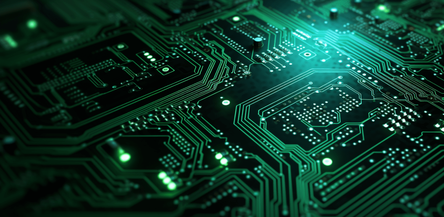
PCB layer stack-up refers to the arrangement of conductive and insulating layers within a multilayer PCB. In high-speed designs, proper stack-up helps minimize signal loss, prevent crosstalk between adjacent traces, and control EMI. The structure typically alternates between signal layers (for routing) and plane layers (for power and ground). Each layer’s role contributes to the overall performance of the PCB, making careful planning essential for high-frequency and high-speed applications.
Why Layer Stack-Up Matters in High-Speed Designs
High-speed signals travel at frequencies where even small design flaws can cause significant performance issues. Signal reflections, timing delays, and interference can arise without a well-structured stack-up. An advanced layer stack-up not only maintains signal integrity but also improves power delivery, reduces noise, and enhances EMI shielding.
Some key considerations for high-speed designs include:
Controlling Impedance: Ensures signal integrity across high-frequency traces.
Minimizing Crosstalk: Reduces noise between adjacent signal lines.
Managing Power Integrity: Maintains stable voltage throughout the PCB.
EMI Mitigation: Prevents electromagnetic interference from affecting signals.
Key Advanced Layer Stack-Up Strategies
Dedicated Ground and Power Plane Layers
Incorporating dedicated ground and power planes is essential for high-speed PCBs. A ground plane provides a low-impedance return path for signals, which is critical for minimizing noise. Having a power plane adjacent to a ground plane helps create a capacitive effect, stabilizing power distribution and reducing voltage fluctuations.
Strategy:
- Place the ground plane directly beneath signal layers to ensure the shortest return path.
- Use adjacent ground and power planes to create distributed capacitance for noise filtering.
Symmetrical Layer Stack-Up
A symmetrical stack-up ensures even distribution of mechanical stress during manufacturing, preventing warping or distortion of the board. In high-speed designs, symmetry also ensures consistent impedance across layers, contributing to uniform signal transmission.
Strategy:
- Maintain symmetry by mirroring the top and bottom layers of the board.
- Balance the number of signal and plane layers to ensure structural stability.
Buried and Blind Vias for Optimized Routing
Buried and blind vias are used to connect inner layers without going through the entire board. These vias help optimize routing, especially in dense, multi-layer designs, by freeing up space on the outer layers for critical signal paths.
Strategy:
- Use blind vias to connect surface layers with internal layers.
- Utilize buried vias to route signals between inner layers without affecting external routing.
Controlled Impedance Layers
Maintaining controlled impedance is crucial in high-speed designs to prevent signal distortion. Impedance control is achieved by carefully managing the thickness of dielectric layers, trace width, and spacing between layers.
Strategy:
- Use tools to calculate trace width and spacing for desired impedance values.
- Place differential pairs on adjacent layers to maintain impedance consistency for high-frequency signals.
Signal Layer Pairing and Routing Guidelines
Pairing high-speed signal layers and routing them in orthogonal directions minimizes crosstalk between traces. Signal layers paired with ground planes also enhance signal integrity by providing a stable return path.
Strategy:
- Pair adjacent signal layers and route them in perpendicular directions (e.g., X-direction on one layer, Y-direction on the next).
- Avoid placing parallel traces on adjacent layers to reduce coupling.
Mitigating EMI with Advanced Stack-Up Techniques
Electromagnetic interference (EMI) can degrade the performance of high-speed PCBs, especially in applications with dense circuitry. An optimized layer stack-up can act as an effective EMI shield.
Strategies:
- Use multiple ground planes to shield critical signal layers.
- Place power and ground planes next to each other to create a Faraday cage effect, minimizing EMI.
- Keep high-speed signals on inner layers, shielded by outer planes.
Thermal Management Through Layer Stack-Up
High-speed PCBs generate more heat due to their increased power consumption. An optimized stack-up helps dissipate heat more effectively by spreading it across multiple layers.
Strategy:
- Use thermal vias to transfer heat from the surface to the inner layers.
- Ensure that power planes are properly distributed to avoid thermal hotspots.
- Incorporate metal-backed layers if the application requires additional heat dissipation.
Prototyping and Testing High-Speed Layer Stack-Ups
Prototyping is essential to validate the effectiveness of the layer stack-up in high-speed PCBs. Top circuit board designers and manufacturers, like FS Circuits, run simulations to predict signal integrity, power distribution, and EMI performance.
Signal Integrity Testing: Use tools like Time-Domain Reflectometry (TDR) to measure impedance across traces.
EMI Testing: Conduct electromagnetic compatibility (EMC) tests to ensure the board meets industry standards.
Thermal Testing: Measure heat distribution to identify potential hotspots.
Applications of Advanced Layer Stack-Up in High-Speed Designs
These advanced stack-up strategies are employed across various high-performance applications:
5G Technology: High-speed communication systems require multi-layer
PCBs with precise impedance control and EMI shielding.
Automotive Electronics: Autonomous vehicles demand reliable PCBs for real-time data processing, where signal integrity is critical.
Data Centers: Servers and network devices use high-speed PCBs to handle large volumes of data with minimal latency.
Medical Devices: High-frequency circuits in diagnostic equipment rely on optimized stack-ups to maintain signal quality.